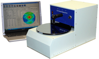
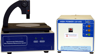
Film Thickness Measurement - ASRM300 Film Thickness Gauge
When you need an accurate thin film thickness measurement our ASRM300 allows you to map film thickness and refractive index up to 5 layers thick. No need to worry about complicated equipment since the ASRM300 is easy to setup and operate. It uses Windows based software, so most people are already familiar with the look and feel of the operating system. This film thickness gauge can handle various types of geometry substrate up to 300mm in diameter and various types of mapping patterns such as linear, polar, square or even arbitrary coordinates. The array based detector system ensures the fastest film thickness measurement. With its advanced optics and rugged design you can always be sure to get the best system performance.
· Easy to set up and operate with Window based software
· Various types of geometry substrate up to 300mm in diameter
· Various types of mapping pattern such as linear, polar, square or arbitrary coordinates
· Advanced optics and rugged design for best system performance
· Array based detector system to ensure fast measurement
· Map film thickness and Refractive Index up to 5 layers
· System comes with comprehensive optical constants database and library
· Include commonly used recipes
· Advanced Software allows user to use either NK table, dispersion or effective media approximation (EMA) for each individual film.
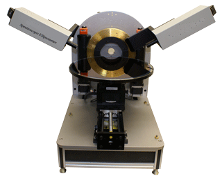
· Upgradeable to AMSP (Microspectrophotometer) mapping system with pattern recognition, or Large Spot for mapping over patterned or featured structure (with Zonerage Model)
· Apply to many different type of substrates with different thickness
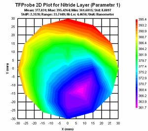
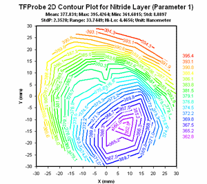
· 2D and 3D output graphics and user friendly data management interface with statistical results
System Configuration:
· Model: SRM300-300
· Detector: CCD Array with 2048 pixels
· Light Source: DC regulated Tungsten-Halogen
· Light Delivery: Optics
· Stage1: Black Anodized Aluminum Alloy Vacuum chuck holds 200 mm wafer
· Communication: USB & RS232
· Software
· Measurement Type: Film thickness, reflection spectrum, refractive index
· Computer: Intel Core 2 Duo Processor with 200GB Hard drive and DVD+RW Burner plus 19 LCD Monitor
· Power: 110 240 VAC /50-60Hz, 3 A
· Dimension: 14(W) x 20(D) x 14(H)
· Weight: 100 lbs
· Warranty: One year labor and parts
Specifications:
Wavelength range: 400 to 1050 nm
Spot Size: 500 µm to 5mm
Sample Size: 300 mm in diameter
Substrate Size: up to 50mm thick
Number of Layers*: Up to 5 films
Measurable thickness range*: 50 nm to 50 µm
Measurement Time: 2ms - 1s /site typical
Positional Repeatability: ~1 µm
Accuracy*: better than 0.5% (comparing with ellipsometry results for Thermal Oxide sample by using the same optical constants)
Repeatability*: < 2? (1 sigma from 50 thickness readings at center for 1500 ? Thermal SiO2 on Si Wafer)
Options:
Additional Models with Wavelength Extension to DUV or NIR Range: ASRM100: 250nm - 1000nm
ASRM400: 900nm - 1700nm
ASRM500: 400nm - 1700nm
Other Sample Size: 200mm wafer (ASRM300-200)
Customized size: Available
Large Spot Accessories for featured structure measurement
Small spot accessories for highly non uniform samples