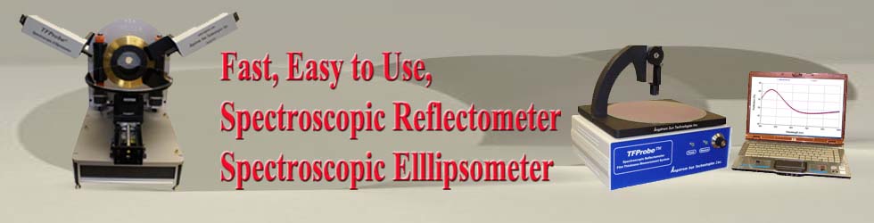
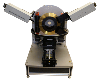
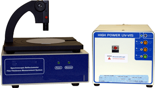
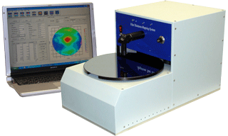
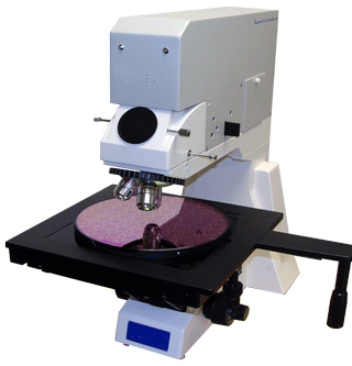
Ellipsometry is an optical technique for the investigation of the dielectric properties of thin films. The E200BA Ellipsometer measures the refractive index and the thickness of semi-transparent thin films. This instrument uses the fact that the reflection at a dielectric interface depends on the polarization of the light while the transmission of light through a transparent layer, changes the phase of the incoming wave depending on the refractive index of the material. Ellipsometers can be used to measure layers as thin as 1 nm up to layers, which are several microns thick. Just one click of a button gives you quick and routine measurements. No external optics are needed to get precise sample alignment interface from the sample signal directly.
When you are looking for a high quality Ellipsometer, the ASE200BA will fulfill your needs.
· Easy to set up
· Easy to operate with Window based software
· Advanced optics design for best system performance
· Automatically change incident angles at 0.01 degree resolution
· High Power DUV-VIS light source for broad band applications
· Array based detector system to ensure fast measurement
· Measure film thickness and Refractive Index up to 12 layers
· Capable to be used for real time or in-line thickness, refractive index monitoring
· System comes with comprehensive optical constants database and library
· Advanced Software allows user to use either NK table, dispersion or effective media approximation (EMA) for each individual film.
· Three different user level control: Engineer mode, system service mode and easy user mode
· Flexible engineer mode for various recipe setup and optical model testing
· Robust one click button (Turn-key) solution for quick and routine measurement
· Configurable measurement parameters, user preference and easiness of operation
· Fully automatic calibration and initialization for system
· Precise sample alignment interface from sample signal directly, no external optics needed
· Precise height and tilting adjustment
· Apply to many different type of substrates with different thickness
· Various options, accessories available for special configurations such as mapping stage, wavelength extension, focus spot etc.
· 2D and 3D output graphics and user friendly data management interface
System Configuration:
· Model: ASE200BA-M300
· Detector: Detector Array
· Light Source: High Power DUV-Vis-NIR Combined Light Source
· Incident Angle Change: Automatic with Program setting
· Stage: Automatic Mapping with Rho-Theta configuration
· Software:
· Computer: Intel Duo Core Processor
· Monitor: 19" Wide Screen LCD
· Power: 110 240 VAC /50-60Hz, 6 A
· Warranty: One year labor and parts
Specifications:
· Wavelength range: 250 to 1000 nm
· Wavelength resolution: 1 nm
· Spot Size: 1 to 5 mm variable
· Incident Angle Range: 10 to 90 degree
· Incident Angle Change Resolution: 0.01 degree
· Sample Size: up to 300 mm in diameter
· Substrate Size: up to 20mm thick
· Measurable thickness range*: 0 nm to 10 µm
· Measurement Time: ~ 1s/Site
· Accuracy*: better than 0.25%
· Repeatability*: < 1 ? (1 sigma from 50 thickness readings for 1500 ? Thermal SiO2 on Si Wafer)
Options:
· Photometry measurement for Reflection and/Or Transmission Measurement
· Micro spot for measuring small area
· Mapping X-Y Stage (X-Y mode, instead of Rho-Theta mode)
· Heating /Cooling Stage
· Vertical Sample Mounting Goniometer
· Wavelength extension to further DUV or IR range
· Scanning Monochromator Setup
· Combined with AMSP for patterned sample measurement with digital imaging functions